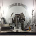
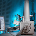
The MRL X-ray Facility provides state-of-the-art x-ray diffraction tools for characterizing structural properties of a wide range of materials including metals and composites, polymers and biological materials, and electronic and optoelectronic materials in the lengthscale range of 0.1 nm - 100 nm. As a key research asset of the MRL, the x-ray facility is accessible by MRL researchers as well as off-campus academic groups and industrial users. In addition to maintaining an array of commercial and custom-built specialty instruments, the facility staff also conducts active research in developing new x-ray imaging methods and instrumentation to advance the capabilities of x-ray characterization techniques.
Facilities
Our group, and the broader nitride group and oxide group, try to perform as much of the experimental work in Shared or Central Facilities at UCSB, including the MBE lab, the Nanofabrication Facility, Microscopy and Microanalysis facility and X-ray Facility.
Equipment
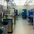
Managed by the Materials Department and open to all members of the university and surrounding community, this facility houses state-of-the-art equipment for materials characterization.
Instruments include 3 transmission electron microscopes, 2 focused ion beam microscopes, 3 field-emission scanning electron microscopes, 4 atomic force microscopes, an atom probe field ion microscope and dedicated XPS and SIMS systems. Advanced sample preparation and computational resources ensure excellent sample quality and high-end data analysis.
The UCSB Nanofabrication facility cleanroom consists of over 12000 ft2 of class 100 and 1000 clean floor space, in a bay and chase configuration, to host a wide variety of thin-film processing equipment. The cleanroom consists of 2 class 100 bays for optical and electron beam lithography and 5 class 1000 bays for other process equipment. A complete description of our tools is available on the equipment web page. A spacious gowning room accomodates up to 350 researchers at any given time and each researcher is given space and utilities for sample and small tool storage. The cleanroom provides bunnysuits, chemicals, source materials for thin film processes, boxes for storage, cleanroom notebooks, and other small ancillaries as part of the recharge rate. Safety procedures and systems are in place to ensure a safe working environment. Training on all systems is required to use our facility. Equipment sign-up is done via a web-based system.
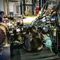
Molecular beam epitaxy (MBE) is a widely used commercial technique for the fabrication of specialised semiconductor devices, particularly those based on III-V materials and used in optoelectronics and high frequency applications. However, it is also a conceptually very simple method of crystal growth. Crystal growth by MBE requires ultra-high vacuum conditions and so MBE is naturally compatible with many surface science techniques. Of particular importance are those techniques which can be operated in situ as growth proceeds - principally reflection high energy electron diffraction (RHEED) and reflection anisotropy spectroscopy (RAS). Other techniques can be employed (e.g. ion scattering, EDX and STM) and practically any surface science tool can be used ex situ by a process of sample transfer under vacuum from the growth chamber.