Research

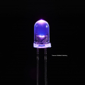
UV LED

Ultraviolet LEDs, particularly at a wavelength of ~280 nm, offer tremendous potential for efficient disinfection for water and air.  Our approach for UV LEDs is based on MOCVD growth on SiC substrates.  We have developed an advanced flip chip process that includes ion etch removal of the SiC growth substrate and subsequent roughening of the AlN [link].  Ongoing work is focused on improving the quality of the AlN buffer layers, active region and developing AlGaN tunnel junctions.

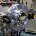
MBE machine

Most GaN-based semiconductors are grown by the outstanding technique:  metalorganic chemical vapor deposition (MOCVD) - an area of great expertise at UCSB.  We also have dedicated activities on molecular beam epitaxy (MBE) growth of group III nitrides.  MBE offers the advantages of an ultrahigh purity environment, in situ characterization by techniques such as reflection high energy electron diffraction (RHEED) and line-of-sight mass desorption spectroscopy, low background concentrations of carbon and hydrogen.  We currently have two dedicated nitride MBEs:  one dedicated to growth with an rf-plasma source for nitrogen (plasma-assisted MBE – PAMBE)and the other with an ammonia (NH3) source for nitrogen.

Picture of LED

Our work on fundaments of group III nitrides includes understanding the impact of natural alloy disorder on carrier localization, transport, and recombination.  In our earlier work with Professor Yuh-Renn Wu (National Taiwan University), we showed that natural alloy disorder in GaN-based LEDs is responsible for the low operating voltage of today’s LEDs, via percolative transport through barriers, and enhanced recombination rates via locally increased carrier density in naturally occurring In-rich regions in InGaN QWs [link

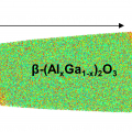
APT picture of Gallium Oxide

β-Ga2O3 is a wide bandgap (4.8 eV) semiconducting oxide that can be grown in high quality single crystals congruently from the melt. Donor doping is relatively easy and there are several options for deep compensating acceptors to produce semi-insulating materials. Due to the predicted breakdown voltage of ~8 MV/cm, the material has great potential for power electron devices. O ur group is focused on PAMBE of β-Ga 2 O 3 and the important β-(AlxGa1-x)2O3 /Ga2O3 heterostructures [link], doping, lateral [link] and vertical devices.

Picture of LED

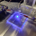
Our main work on visible LEDs has two main aspects.  First, we continue to work to improve the efficiency of blue and green GaN-based LEDs.  Second we work to understand the fundamental causes of inefficiency in GaN-based LEDs:  namely the mechanisms of Shockley-Read-Hall (SRH) recombination and Auger recombination.