Molecular Beam Epitaxy
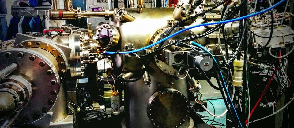
Molecular beam epitaxy (MBE) is a widely used commercial technique for the fabrication of specialised semiconductor devices, particularly those based on III-V materials and used in optoelectronics and high frequency applications. However, it is also a conceptually very simple method of crystal growth. Crystal growth by MBE requires ultra-high vacuum conditions and so MBE is naturally compatible with many surface science techniques. Of particular importance are those techniques which can be operated in situ as growth proceeds - principally reflection high energy electron diffraction (RHEED) and reflection anisotropy spectroscopy (RAS). Other techniques can be employed (e.g. ion scattering, EDX and STM) and practically any surface science tool can be used ex situ by a process of sample transfer under vacuum from the growth chamber.